Gutscheinbedingungen

**Gültig bis 14.09.2026 auf Spielzeug, Schreibwaren, Filme, Geschenke & Trends, Musik, tolino eReader & Zubehör, Hörbücher, nicht preisgebundene Bücher und Kalender in der Thalia App. Einzelne Artikel können ausgeschlossen sein. Aufgrund der Buchpreisbindung sind deutschsprachige Bücher und eBooks ausgenommen. Zusätzlich ausgenommen sind Abos & Flatrates, Games, Geschenkkarten/-boxen, Shelfies, Software, Zeitschriften sowie einzelne Artikel von tonies®. Pro Einkauf einmal einlösbar. Nur gültig mit im Onlineshop hinterlegter Bonuscard. Click & Collect nur bei Onlinevorabzahlung möglich. Keine Barauszahlung. Nicht kombinierbar mit anderen Aktionen und Gutscheinen. Gutschein wird auf max. 500€ Bestellwert angerechnet. Nicht gültig für Versandkosten und Services.

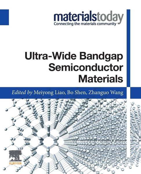
Produktbild: Ultra-wide Bandgap Semiconductor Materials
- 13%

Ultra-wide Bandgap Semiconductor Materials

Aus der Reihe Materials Today
13% sparen

183,99 € UVP 211,80 €

inkl. gesetzl. MwSt., Versandkostenfrei


Beschreibung

Produktdetails

Einband

Taschenbuch

Erscheinungsdatum

28.06.2019

Herausgeber

Meiyong Liao + weitere

Verlag

Elsevier Science & Technology

Seitenzahl

504

Maße (L/B/H)

23,5/19,1/2,6 cm

Gewicht

859 g

Sprache

Englisch

ISBN

978-0-12-815468-7

Beschreibung

Rezension

"This book provides recent progress of the development of new UWBS materials and shows the advantages of these materials over existing WBS materials. It provides in-depth technical details on the latest developments of efficiency, and performance of power UWBS materials as well as device per electronic devices." --IEEE

Portrait

Meiyong Liao received his doctor of Materials Science at the Institute for Semiconductors, Chinese Academy of Science (Beijing, China) 2002. For two years he was a visiting researcher at Kyoto University, Japan. Then, he joined the Diamond Research Group at the National Institute for Materials Science, Tsukuba in 2004. Presently, he works as a principal researcher at NIMS on the topics of semiconducting diamond growth, device physics, and applications. He developed the world-record DUV diamond photodetector and proposed the photoconductive mechanism of diamond. He also proposed a novel type normally-off diamond transistor. He pioneered the semiconductor single crystal diamond MEMS/NEMS and demonstrated the SCD NEMS switch for the first time. He has been engaged in CVD diamond research for more than 15 years and published more than 150 peer-reviewed journal papers with more than 6000 citations.
Dr. Shen is the head and medical director of the IBD Center at Columbia. He is also the Vice Chair for Innovation in Medicine and Surgery and a Professor of Medicine (in Surgery). He is one of the world's pre-eminent leaders in interventional inflammatory bowel disease (IBD) due to his specialized expertise in treating a wide range of pouch-related disorders. In addition to pouchitis and pouch diseases, Dr. Shen specializes in IBD, GI endoscopy (including endoscopic pouch procedures), and imaging technology. Dr. Shen is known as a pioneer in interventional treatment for IBD - this includes postponing or eliminating the need for surgery in some cases.
Zhanguo Wang is a semiconductor materials physicist, and Research Professor in the Institute of Semiconductors, Chinese Academy of Sciences. Zhanguo Wang was elected as a Member of the Chinese Academy of Sciences in 1995. In the early 1960s, Wang was engaged in studies on radiation effects of silicon solar cells for satellites and the optical and electrical properties of semiconductor materials. From 1980, his main interests were on the deep level physics and spectrum physics of semiconductors. He and his colleagues developed a new method to identify whether the two deep levels within a band gap are coupled or not, thus solving the long existing fundamental question of gold-related donor and acceptor in Si, and A and B deep levels in LPE GaAs. He suggested a model of deep level broadening and PL spectrum splitting in semiconductor alloys. In 1986, he joined Professor Lin Lanying's group, and the GaAs single crystal was successfully grown from the melt in space for the first time. In 1993, he proposed a multi-level compensation model and new criteria of electrical compensation for undoped SI-GaAs, which can not only explain the GaAs conductivity but also provide a clue for improving the quality of this material. Recently, he and his co-workers are working on low dimensional semiconductor materials (quantum well, quantum wires and quantum dots etc) growth and quantum devices fabrication. His group has also been engaged in the research of wide-band gap semiconductors of III-nitrides, ZnO, diamond, BN, etc. He has published more than 400 peer-reviewed journal papers and is the author of several academic books.

Produktdetails

Einband

Taschenbuch

Erscheinungsdatum

28.06.2019

Herausgeber

Verlag

Elsevier Science & Technology

Seitenzahl

504

Maße (L/B/H)

23,5/19,1/2,6 cm

Gewicht

859 g

Sprache

Englisch

ISBN

978-0-12-815468-7

Herstelleradresse

Libri GmbH
Europaallee 1
36244 Bad Hersfeld
DE

Email: gpsr@libri.de

Noch keine Bewertungen vorhanden

Verfassen Sie die erste Bewertung zu diesem Artikel

Helfen Sie anderen Kundinnen und Kunden durch Ihre Meinung.

Kundinnen und Kunden meinen

Bewertungen (0)

Die Leseprobe wird geladen.
  • Produktbild: Ultra-wide Bandgap Semiconductor Materials
  • 1. Al-rich AlGaN semiconductor materials and their device applications
    2. Semiconductor diamond
    > Progress in semiconductor ß-Ga2O3
    4. Recent progress of boron nitrides
    5. Nanostructures based on UWBG materials