KI-Beratung Beta

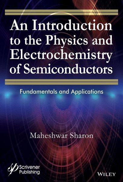
Produktbild: An Introduction to the Physics and Electrochemistry of Semiconductors

An Introduction to the Physics and Electrochemistry of Semiconductors Fundamentals and Applications

247,99 €

inkl. gesetzl. MwSt., Versandkostenfrei


Beschreibung

Produktdetails

Einband

Gebundene Ausgabe

Erscheinungsdatum

19.09.2016

Verlag

John Wiley & Sons Inc

Seitenzahl

352

Maße (L/B/H)

23,1/15,5/2,5 cm

Gewicht

680 g

Auflage

1. Auflage

Sprache

Englisch

ISBN

978-1-119-27433-9

Beschreibung

Produktdetails

Einband

Gebundene Ausgabe

Erscheinungsdatum

19.09.2016

Verlag

John Wiley & Sons Inc

Seitenzahl

352

Maße (L/B/H)

23,1/15,5/2,5 cm

Gewicht

680 g

Auflage

1. Auflage

Sprache

Englisch

ISBN

978-1-119-27433-9

Herstelleradresse

Libri GmbH
Europaallee 1
36244 Bad Hersfeld
DE

Email: gpsr@libri.de

Noch keine Bewertungen vorhanden

Verfassen Sie die erste Bewertung zu diesem Artikel

Helfen Sie anderen Kundinnen und Kunden durch Ihre Meinung.

Kundinnen und Kunden meinen

Bewertungen (0)

Die Leseprobe wird geladen.
  • Produktbild: An Introduction to the Physics and Electrochemistry of Semiconductors
  • Foreword xv
     
    Preface xvii
     
    1 Our Universe and the Sun 1
     
    1.1 Formation of the Universe 1
     
    1.2 Formation of Stars 2
     
    1.2.1 Formation of Energy in the Sun 3
     
    1.2.2 Description of the Sun 6
     
    1.2.3 Transfer of Solar Rays through the Ozone Layer 6
     
    1.2.4 Transfer of Solar Layers through Other Layers 7
     
    1.2.5 Effect of Position of the Sun vis-à-vis the Earth 8
     
    1.2.6 Distribution of Solar Energy 8
     
    1.2.7 Solar Intensity Calculation 8
     
    1.3 Summary 12
     
    Reference 12
     
    2 Solar Energy and Its Applications 13
     
    2.1 Introduction to a Semiconductor 14
     
    2.2 Formation of a Compound 14
     
    2.2.1 A Classical Approach 14
     
    2.2.2 Why Call It a Band and Not a Level? 15
     
    2.2.3 Quantum Chemistry Approach 17
     
    2.2.3.1 Wave Nature of an Electron in a Fixed Potential 17
     
    2.2.3.2 Wave Nature of an Electron under a Periodically Changing Potential 19
     
    2.2.3.3 Bloch's Solution to the Wave Function of Electrons under Variable Potentials 20
     
    2.2.3.3 Concept of a Forbidden Gap in a Material 22
     
    2.2.4 Band Model to Explain Conductivity in Solids 25
     
    2.2.4.1 Which of the Total Electrons Will Accept the External Energy for Their Excitation? 26
     
    2.2.4.2 Density of States 28
     
    2.2.4.3 How Do We Find the Numbers of Electrons in These Bands? 29
     
    2.2.5 Useful Deductions 31
     
    2.2.5.1 Extrinsic Semiconductor 33
     
    2.2.5.2 Role of Dopants in the Semiconductor 36
     
    2.3 Quantum Theory Approach to Explain the Effect of Doping 37
     
    2.3.1 A Mathematical Approach to Understanding This Problem 39
     
    2.3.2 Representation of Various Energy Levels in a Semiconductor 40
     
    2.4 Types of Carriers in a Semiconductor 42
     
    2.4.1 Majority and Minority Carriers 42
     
    2.4.2 Direction of Movement of Carriers in a Semiconductor 42
     
    2.5 Nature of Band Gaps in Semiconductors 44
     
    2.6 Can the Band Gap of a Semiconductor Be Changed? 45
     
    2.7 Summary 47
     
    Further Reading 47
     
    3 Theory of Junction Formation 49
     
    3.1 Flow of Carriers across the Junction 49
     
    3.1.1 Why Do Carriers Flow across an Interface When n- and p-Type Semiconductors Are Joined Together with No Air Gap? 49
     
    3.1.2 Does the Vacuum Level Remain Unaltered, and What Is the Significance of Showing a Bend in the Diagram? 52
     
    3.1.3 Why Do We Draw a Horizontal or Exponential Line to Represent the Energy Level in the Semiconductor with a Long Line? 52
     
    3.1.4 What Are the Impacts of Migration of Carriers toward the Interface? 52
     
    3.2 Representing Energy Levels Graphically 54
     
    3.3 Depth of Charge Separation at the Interface of n- and p-Type Semiconductors 56
     
    3.4 Nature of Potential at the Interface 56
     
    3.4.1 Does Any Current Flow through the Interface? 56
     
    3.4.2 Effect of Application of External Potential to the p:n Junction Formed by the Two Semiconductors 58
     
    3.4.2.1 Flow of Carriers from n-Type to p-Type 59
     
    3.4.2.2 Flow of Carriers from p-Type to n-Type 60
     
    3.4.2.3 Flow of Current due to Holes 60
     
    3.4.2.4 Flow of Current due to Electrons 61
     
    3.4.3 What Would Happen If Negative Potential Were Applied to a p-Type Semiconductor? 62
     
    3.4.3.1 Flow of Majority Carriers from p- to n-Type Semiconductors 63
     
    3.4.3.2 Flow of Majority Carriers from n- to p-Type 63
     
    3.4.3.3 Flow of Minority Carrier from p- to n-Type Semiconductors 64
     
    3.4.3.3 Flow of Minority Carriers from n- to p-Type Semiconductors 64
     
    3.5 Expression for Saturation (or Exchange) Curre