KI-Beratung Beta

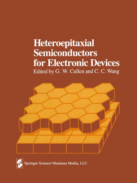
  • Produktbild: Heteroepitaxial Semiconductors for Electronic Devices
  • Produktbild: Heteroepitaxial Semiconductors for Electronic Devices

Heteroepitaxial Semiconductors for Electronic Devices

99,99 €

inkl. gesetzl. MwSt., Versandkostenfrei


Beschreibung

Some years ago it was not uncommon for materials scientists, even within the electronics industry, to work relatively independently of device engi neers. Neither group had a means to determine whether or not the materials had been optimized for application in specific device structures. This mode of...

Beschreibung

Some years ago it was not uncommon for materials scientists, even within the electronics industry, to work relatively independently of device engi neers. Neither group had a means to determine whether or not the materials had been optimized for application in specific device structures. This mode of operation is no longer desirable or possible. The introduction of a new material, or a new form of a well known material, now requires a close collaborative effort between individuals who represent the disciplines of materials preparation, materials characterization, device design and pro cessing, and the analysis of the device operation to establish relationships between device performance and the materials properties. The develop ment of devices in heteroepitaxial thin films has advanced to the present state specifically through the unusually close and active interchange among individuals with the appropriate backgrounds. We find no book available which brings together a description of these diverse disciplines needed for the development of such a materials-device technology. Therefore, the authors of this book, who have worked in close collaboration for a number of years, were motivated to collect their experiences in this volume. Over the years there has been a logical flow of activity beginning with heteroepi taxial silicon and progressing through the III-V and II-VI compounds. For each material the early emphasis on material preparation and characteriza tion later shifted to an emphasis on the analysis of the device characteristics specific to the materials involved.

Produktdetails

Einband

Taschenbuch

Erscheinungsdatum

28.08.2013

Abbildungen

XIII, 299 p. 54 illus.

Herausgeber G.W. Cullen + weitere

Produktdetails

Einband

Taschenbuch

Erscheinungsdatum

28.08.2013

Abbildungen

XIII, 299 p. 54 illus.

Herausgeber
Verlag Springer Us
Seitenzahl

299

Maße (L/B/H)

27,9/21/1,8 cm

Gewicht

774 g

Auflage

Softcover reprint of the original 1st ed. 1978

Sprache

Englisch

ISBN

978-1-4612-6269-5

Herstelleradresse

Springer-Verlag KG
Sachsenplatz 4-6
1201 Wien
AT

Email: ProductSafety@springernature.com

Noch keine Bewertungen vorhanden

Verfassen Sie die erste Bewertung zu diesem Artikel

Helfen Sie anderen Kundinnen und Kunden durch Ihre Meinung.

Kundinnen und Kunden meinen

Bewertungen (0)

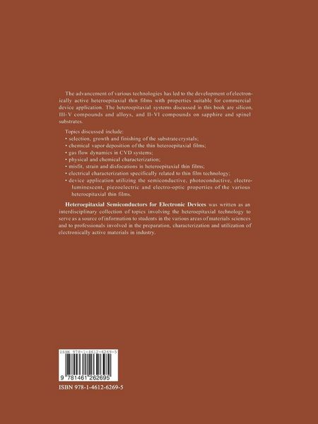
  • Produktbild: Heteroepitaxial Semiconductors for Electronic Devices
  • Produktbild: Heteroepitaxial Semiconductors for Electronic Devices