KI-Beratung Beta

  • Produktbild: Electrical Characterization of Silicon-on-Insulator Materials and Devices
  • Produktbild: Electrical Characterization of Silicon-on-Insulator Materials and Devices
Band 305 - 12%

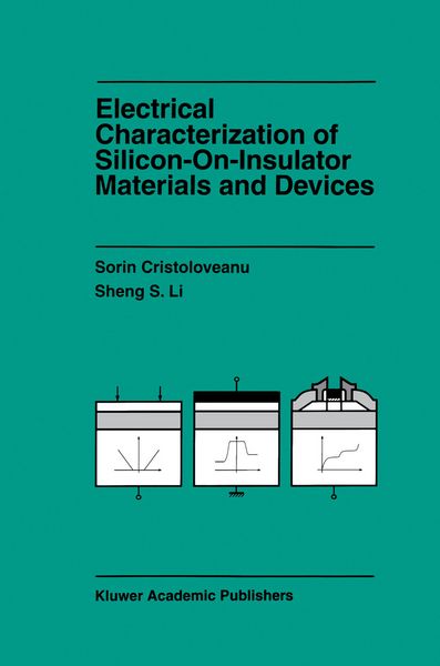
Electrical Characterization of Silicon-on-Insulator Materials and Devices

12% sparen

192,99 € UVP 219,99 €

inkl. gesetzl. MwSt., Versandkostenfrei


Beschreibung

Produktdetails

Einband

Gebundene Ausgabe

Erscheinungsdatum

30.06.1995

Abbildungen

XV, 381 p.

Verlag

Springer Us

Seitenzahl

381

Maße (L/B/H)

24,1/16/2,6 cm

Gewicht

764 g

Auflage

1995 edition

Sprache

Englisch

ISBN

978-0-7923-9548-5

Beschreibung

Produktdetails

Einband

Gebundene Ausgabe

Erscheinungsdatum

30.06.1995

Abbildungen

XV, 381 p.

Verlag

Springer Us

Seitenzahl

381

Maße (L/B/H)

24,1/16/2,6 cm

Gewicht

764 g

Auflage

1995 edition

Sprache

Englisch

ISBN

978-0-7923-9548-5

Herstelleradresse

Libri GmbH
Europaallee 1
36244 Bad Hersfeld
DE

Email: gpsr@libri.de

Noch keine Bewertungen vorhanden

Verfassen Sie die erste Bewertung zu diesem Artikel

Helfen Sie anderen Kundinnen und Kunden durch Ihre Meinung.

Kundinnen und Kunden meinen

Bewertungen (0)

  • Produktbild: Electrical Characterization of Silicon-on-Insulator Materials and Devices
  • Produktbild: Electrical Characterization of Silicon-on-Insulator Materials and Devices
  • Preface.- 1 Introduction.- 1.1 Why SOI ?.- 1.2 Why Not Yet SOI ?.- 1.3 Why an SOI Book?.- 2 Methods of Forming SOI Wafers.- 2.1 SIMOX.- 2.2 Wafer Bonding.- 2.3 Zone-Melting Recrystallization.- 2.4 Epitaxial Lateral Overgrowth.- 2.5 Full Isolation by Porous Oxidized Silicon.- 2.6 Silicon on Sapphire.- 2.7 Silicon on Zirconia.- 3 SOI Devices.- 3.1 Advanced CMOS and Bipolar Devices.- 3.2 Radiation-Hardened Circuits.- 3.3 High-Voltage Devices.- 3.4 High-Temperature Devices.- 3.5 Low-Power Applications.- 3.6 Three-Dimensional Devices.- 3.7 Transducers.- 3.8 Innovative Devices.- 4 Wafer-Screening Techniques.- 4.1 The Basis for Wafer Screening.- 4.2 Surface Photovoltage.- 4.3 Dual-Beam S-Polarized Reflectance.- 4.4 Dual-Beam Optical Modulation.- 4.5 Other Optical Methods.- 4.6 Point Contact Pseudo-MOS Transistor.- 4.7 Quick-Turnaround Capacitance.- 4.8 Pinhole Detection.- 4.9 Conclusion.- 5 Transport Measurements.- 5.1 Four-Point Probe.- 5.2 Spreading Resistance.- 5.3 Hall Effect and Magnetoresistance.- 5.4 Van der Pauw Measurements.- 5.5 Photoconductivity.- 5.6 PICTS.- 6 SIS Capacitor-Based Characterization Techniques.- 6.1 Capacitance and Conductance Techniques.- 6.2 Bias-Scan DLTS Technique.- 6.4 Zerbst Method and Generation Lifetime.- 6.5 MOS Capacitance Method.- 7 Diode Measurements.- 7.1 Current—Voltage Measurements in a P—N Diode.- 7.2 Differential Current/Capacitance Method.- 7.3 Gated-Diode Measurements.- 7.4 Deep-Level Transient Spectroscopy.- 8 Electrical Characterization of SOI Materials and Devices MOS Transistor Characteristics.- 9 Transistor-Based Characterization Techniques.- List of Symbols.